The latest differences in laser confocal microscopy, scanning electron microscopy, and atomic force microscopy
Laser confocal microscopy, scanning electron microscopy, and atomic force microscopy are relatively many imaging systems currently used in scientific research. In recent years, with the continuous development of technology, various system-related applications have become a trend. This paper simply sorts out the differences and related progress of various microscopes. First , the limit resolution is different, due to the difference of the amplified signal source <br> Laser confocal: limit resolution 150nm. Using ultra-thin monochrome short-wave visible light for light source imaging, the resolution and image quality can be changed by changing the objective lens.
Scanning electron microscopy: According to the principle of electron gun emission, the current technology has a limit resolution of 20nm~0.8nm. Electron optical imaging is used. The resolution is changed mainly by changing the focal length of the electromagnetic lens.
Atomic Force Microscopy: 0.1nm limit resolution, lever-amplified laser ranging imaging! The radius of curvature of the scanning tip determines the resolution.
Second , the scanning drive method is different <br> Laser confocal: the laser source is very thin, using a computer-controlled laser mirror to control the laser scanning range and scanning speed, thereby controlling the magnification and image quality.
Scanning Electron Microscope: A computer-controlled scanning coil controls the electron beam scanning range and scanning speed to adjust the magnification and image quality.
Atomic Force Microscopy: A computer-controlled piezoelectric displacement sensor drives the X- and Y-direction scans of the sample stage to achieve scan range and scan speed control, thereby changing magnification and image quality.
Third, the difference between stereo imaging <br> Laser confocal: through the nano-precision stepper motor to drive the sample in the Z-axis direction layer by layer imaging, and then the software will set the layers of the image into a clear stereo image.
Image depth of field is determined by the Z-week drive range.
Scanning electron microscope: A single-frame image has a large depth of field, but it belongs to a two-dimensional image, and three-dimensional imaging can be realized by stereo pair technology.
Atomic Force Microscopy: The essence of imaging is to measure the height of each pixel on the surface, depicting the three-dimensional appearance. Therefore, the data in the Z direction of each pixel must be accurate, otherwise the shape is not accurate. Traditionally, a tubular driver is used, and the X/Y direction is swung and scanned, resulting in image distortion and poor reproducibility. The latest use of independent X, Y scan driver, accurate appearance.
Fourth, the difference in working environment <br> Laser confocal and atomic force microscopy can be tested in the atmosphere. General scanning electron microscope must be tested under high vacuum conditions
V. Differences in application range <br> Laser confocal: several times ~ several thousand times, sample preparation is simple Scanning electron microscopy: several times ~ several hundred thousand times, sample preparation is slightly more complicated, but the overall is also very simple atomic force microscope: tens of thousands of times ~ tens of millions of times, the sample is required to be very flat and sample preparation is difficult. For example, A4 paper is too rough to be observed.
System related developments
Laser confocal is associated with scanning electron microscopy. Zeiss's SHUTTER & FIND launched in 2013 can integrate laser confocal and scanning electron microscopy, and several other brands have collaborated to launch such systems.
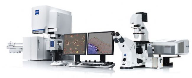
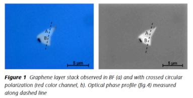
Application example - Study of graphene characteristics by scanning electron microscopy and white confocal microscopy
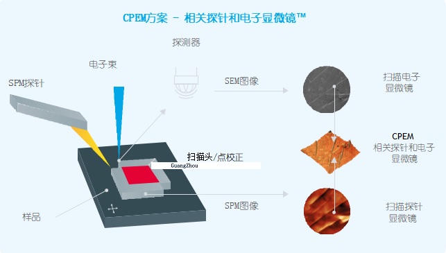
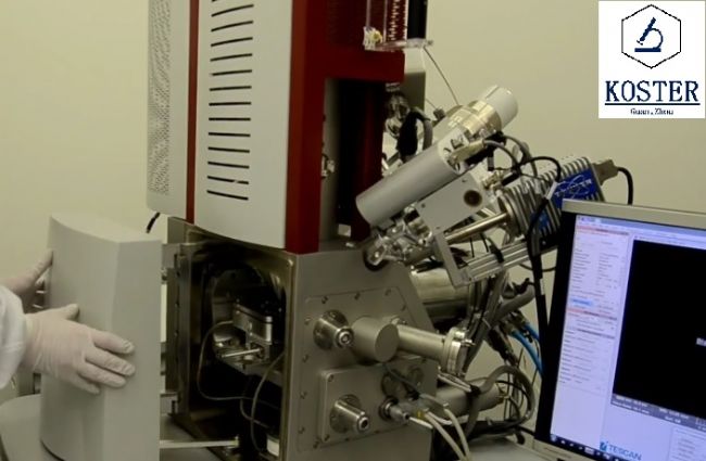
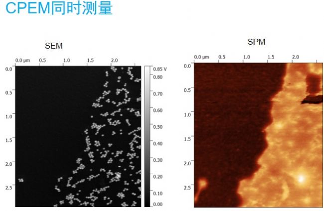
AFM and SEM SEM imaging (CPEM)
Nenovision, a Czech atomic microscope manufacturer, launched the litescope in 2016, and the patented CPEM technology has been tested on ZEISS, FEI, Nippon Electronics, Tescan and other electronic mirror platforms. The system has been sold in Europe.
Integrates the technical advantages of AFM and SEM, a plug-and-play solution – easy to use and easy to use
SEM – image, chemical analysis, surface modification
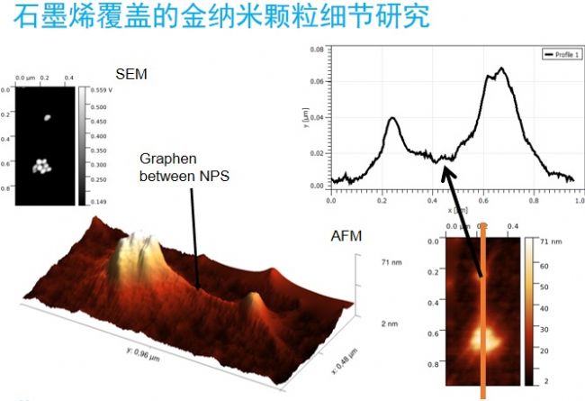
AFM – 3D surface topography, roughness, electrical conductivity, electronic properties
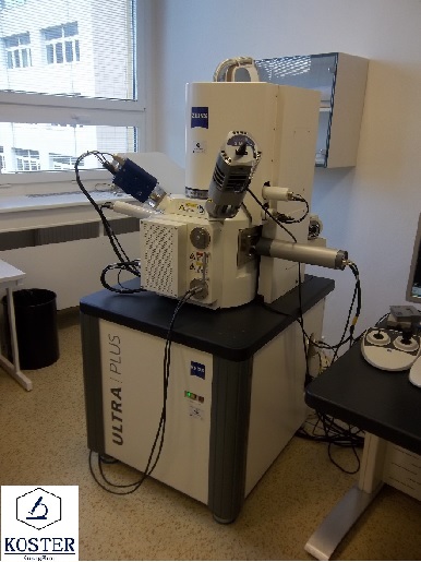
Application example: Detail study of graphene-coated gold nanoparticles
Medical Caps,Non-woven Medical Caps,Protective Medical Caps,Protective Non-woven Caps,Disposable Medical Caps,Disposable Non-woven Caps
Medical Caps,Non-woven Medical Caps,Protective Medical Caps,Protective Non-woven Caps,Disposable Medical Caps,Disposable Non-woven Caps
Luck Medical Consumables Co.,LIMITED , https://www.luckmedical.com